


Epson Research and Development Page 13
Vancouver Design Center
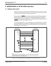
Interfacing to the Motorola MC68VZ328 Dragonball Microprocessor S1D13708
Issue Date: 01/11/25 X39A-G-016-01
4.2.1 Register/Memory Mapping
The S1D13708 requires two 128K byte segments in memory for the display buffer and its
internal registers. To accommodate this block size, it is preferable (but not required) to use
one of the chip selects from groups A or B. Groups A and B can have a size range of 128K
bytes to 16M bytes and groups C and D have a size range of 32K bytes to 16M bytes.
Therefore, any chip select other than CSA0 would be suitable for the S1D13708 interface.
In the example interface, chip select CSB1 controls the S1D13708. A 256K byte address
space is used with the S1D13708 internal registers occupying the first 128K byte block and
the 80K byte display buffer located in the second 128K byte block. A17 from the
MC68VZ328 is used to select between these two 128K byte blocks.
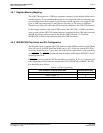
4.2.2 MC68VZ328 Chip Select and Pin Configuration
The chip select used to map the S1D13708 (in this example CSB1) must have its RO (Read
Only) bit set to 0, its BSW (Bus Data Width) set to 1 for a 16-bit bus, and the WS (Wait
states) bits should be set to 111b to allow the S1D13708 to terminate bus cycles externally
with DTACK
. The DTACK pin function must be enabled with Register FFFFF433, Port G
Select Register, bit 0.
If DTACK
is not used, then the WS bits should be set to either 4, 6, 10, or 12 software wait
states depending on the divide ratio between the S1D13708 MCLK and BCLK. The WS
bits should be set as follows.
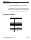
Table 4-3: WS Bit Programming
S1D13708 MCLK to BCLK Divide Ratio WS Bits (wait states)
MCLK = BCLK 6
MCLK = BCLK ÷ 29
MCLK = BCLK ÷ 312