


Epson Research and Development Page 153
Vancouver Design Center
Hardware Functional Specification S1D13708
Issue Date: 02/03/07 X39A-A-001-02
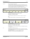
bit 0 PWMCLK Source Select
When this bit = 0, the clock source for PWMCLK is the BCLK source.
When this bit = 1, the clock source for PWMCLK is CLKI2 or XTAL (see BCLK Source
Select Register on page 157).
Note
For further information on the PWMCLK source select, see Section 7.2, “Clock Selec-
tion” on page 116.
bits 7-0 CV Pulse Burst Length Bits [7:0]
The value of this register determines the number of pulses generated in a single CV Pulse
burst:
Number of pulses in a burst = (ContentsOfThisRegister) + 1
bits 7-0 PWMOUT Duty Cycle Bits [7:0]
This register determines the duty cycle of the PWMOUT output.
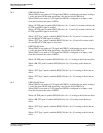
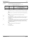
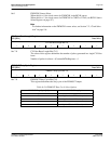
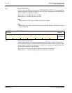
CV Pulse Burst Length Register
REG[B2h] Read/Write
CV Pulse Burst Length Bits 7-0
76543210
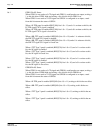
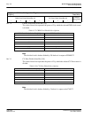
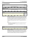
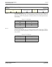
PWMOUT Duty Cycle Register
REG[B3h] Read/Write
PWMOUT Duty Cycle Bits 7-0
76543210
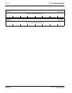
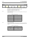
Table 8-19: PWMOUT Duty Cycle Select Options
PWMOUT Duty Cycle [7:0] PWMOUT Duty Cycle
00h Always Low
01h High for 1 out of 256 clock periods
02h High for 2 out of 256 clock periods
... ...
FFh High for 255 out of 256 clock periods