


Epson Research and Development Page 43
Vancouver Design Center
Hardware Functional Specification S1D13708
Issue Date: 02/03/07 X39A-A-001-02
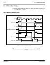
Note
Maximum internal requirements for clocks derived from CLKI must be considered
when determining the frequency of CLKI. See Section 6.1.2, “Internal Clocks” on page
43 for internal clock requirements.
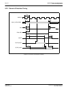
Note
Maximum internal requirements for clocks derived from CLKI2 must be considered
when determining the frequency of CLKI2. See Section 6.1.2, “Internal Clocks” on page
43 for internal clock requirements.
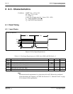
6.1.2 Internal Clocks
Note
For further information on internal clocks, refer to Section 7, “Clocks” on page 112.
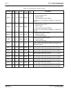
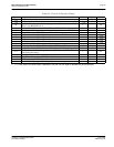
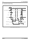
Table 6-2: Clock Input Requirements for CLKI when CLKI to BCLK divide = 1
Symbol Parameter Min Max Units
f
OSC
Input Clock Frequency (CLKI) 66 MHz
T
OSC
Input Clock period (CLKI) 1/f
OSC
ns
t
PWH
Input Clock Pulse Width High (CLKI) 3 ns
t
PWL
Input Clock Pulse Width Low (CLKI) 3 ns
t
f
Input Clock Fall Time (10% - 90%) 5 ns
t
r
Input Clock Rise Time (10% - 90%) 5 ns
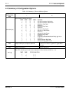
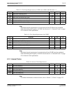
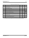
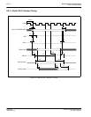
Table 6-3: Clock Input Requirements for CLKI2
Symbol Parameter Min Max Units
f
OSC
Input Clock Frequency (CLKI2) 66 MHz
T
OSC
Input Clock period (CLKI2) 1/f
OSC
ns
t
PWH
Input Clock Pulse Width High (CLKI2) 3 ns
t
PWL
Input Clock Pulse Width Low (CLKI2) 3 ns
t
f
Input Clock Fall Time (10% - 90%) 5 ns
t
r
Input Clock Rise Time (10% - 90%) 5 ns
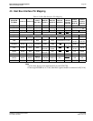
Table 6-4: Internal Clock Requirements
Symbol Parameter Min Max Units
f
BCLK
Bus Clock frequency 66 MHz
f
MCLK
Memory Clock frequency 50 MHz
f
PCLK
Pixel Clock frequency 50 MHz
f
PWMCLK
PWM Clock frequency 66 MHz
f
XTAL
XTAL Clock frequency 12 MHz