


Page 32 Epson Research and Development
Vancouver Design Center
S1D13708 Hardware Functional Specification
X39A-A-001-02 Issue Date: 02/03/07
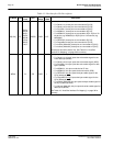
RD/WR# I B3 PIC IOVDD 1
This input pin has multiple functions.
• For Generic #1, this pin inputs the read command for the upper
data byte (RD1#).
• For Generic #2, this pin must be tied to IO V
DD
.
• For SH-3/SH-4, this pin inputs the RD/WR# signal. The
S1D13708 needs this signal for early decode of the bus cycle.
• For MC68K #1, this pin inputs the R/W# signal.
• For MC68K #2, this pin inputs the R/W# signal.
• For REDCAP2, this pin inputs the R/W signal.
• For DragonBall, this pin must be tied to IO V
DD
.
• For Indirect (Mode 68), this pin inputs the R/W# signal.
• For Indirect (Mode 80, this pin inputs the read enable signal for
data byte 0 (RDL#).
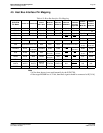
See Table 4-9: “Host Bus Interface Pin Mapping,” on page 39
for
summary.
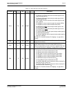
RD# I H7 PIC IOVDD 1
This input pin has multiple functions.
• For Generic #1, this pin inputs the read command for the lower
data byte (RD0#).
• For Generic #2, this pin inputs the read command (RD#).
• For SH-3/SH-4, this pin inputs the read signal (RD#).
• For MC68K #1, this pin must be tied to IO V
DD
.
• For MC68K #2, this pin inputs the bus size bit 1 (SIZ1).
• For REDCAP2, this pin inputs the output enable (OE
).
• For DragonBall, this pin inputs the output enable (OE).
• For Indirect (Mode 68), this pin is tied to V
SS
.
• For Indirect (Mode 80), this pin inputs the read enable signal for
data byte 1 (RDU#).
See Table 4-9: “Host Bus Interface Pin Mapping,” on page 39
for
summary.
Table 4-3: Host Interface Pin Descriptions
Pin Name Type
PFBGA
Pin #
Cell
IO
Voltage
RESET
# State
Description