Page 66 Epson Research and Development
Vancouver Design Center
S1D13708 Hardware Functional Specification
X39A-A-001-02 Issue Date: 02/03/07
6.3 LCD Power Sequencing
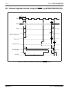
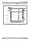
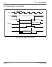
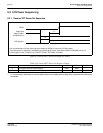
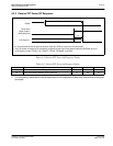
6.3.1 Passive/TFT Power-On Sequence
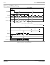
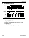
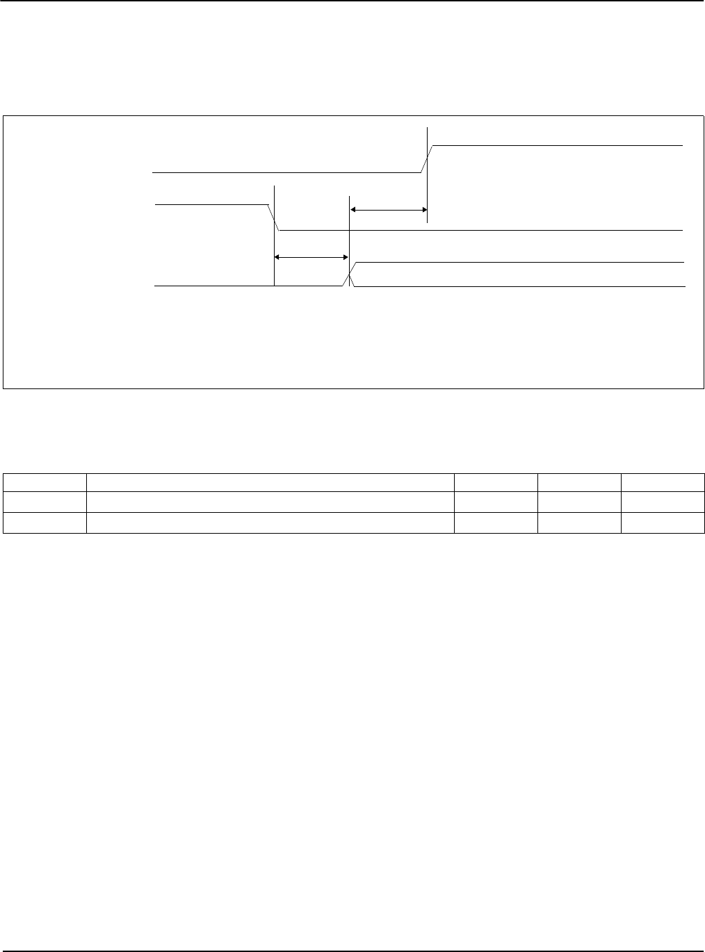
Figure 6-13 Passive/TFT Power-On Sequence Timing
1. t1 is controlled by software and must be determined from the bias power supply delay requirements of the panel
connected.
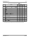
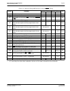
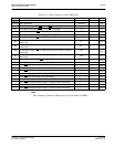
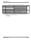
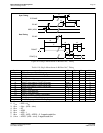
Table 6-16: Passive/TFT Power-On Sequence Timing
Symbol Parameter Min Max Units
t1
LCD signals active to LCD bias active
Note 1 Note 1
t2
Power Save Mode disabled to LCD signals active
020ns
LCD Signals***
GPO0*
Power Save
t1
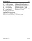
*It is recommended to use the general purpose output pin GPO0 to control the LCD bias power.
t2
**The LCD power-on sequence is activated by programming the Power Save Mode Enable bit (REG[A0h] bit 0) to 0.
***LCD Signals include: FPDAT[17:0], FPSHIFT, FPLINE, FPFRAME, and DRDY.
(REG[A0h] bit 0)
Mode Enable**


