


Page 146 Epson Research and Development
Vancouver Design Center
S1D13708 Hardware Functional Specification
X39A-A-001-02 Issue Date: 02/03/07
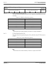
bit 7 GPIO Pin Input Enable
This bit is used to enable the input function of the GPIO pins. It must be changed to a 1
after power-on reset to enable the input function of the GPIO pins (default is 0).
Note
For information on GPIO pin mapping when HR-TFT/D-TFD panels are selected, see
Table 4-10: “LCD Interface Pin Mapping,” on page 40.
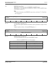
bit 6 GPIO6 Pin IO Status
When GPIO6 is not used as a LCD signal and GPIO6 is configured as an output, writing a
1 to this bit drives GPIO6 high and writing a 0 to this bit drives GPIO6 low.
When GPIO6 is not used as a LCD signal and GPIO6 is configured as an input, a read
from this bit returns the status of GPIO6.
When a D-TFD panel is enabled (REG[10h] bits 1:0 = 11) writing to this bit has no effect.
When a TFT Type 3 panel is enabled (REG[C5h] bits 1:0 = 10) writing to this bit has no
effect.
bit 5 GPIO5 Pin IO Status
When GPIO5 is not used as a LCD signal and GPIO5 is configured as an output, writing a
1 to this bit drives GPIO5 high and writing a 0 to this bit drives GPIO5 low.
When GPIO5 is not used as a LCD signal and GPIO5 is configured as an input, a read
from this bit returns the status of GPIO5.
When a D-TFD panel is enabled (REG[10h] bits 1:0 = 11) and a 1 is written to this bit, the
D-TFD signal DD_P1 signal is enabled.
When a D-TFD panel is enabled (REG[10h] bits 1:0 = 11) and a 0 is written to this bit, the
D-TFD signal DD_P1 signal is forced low.
When a TFT Type 3 panel is enabled (REG[C5h] bits 1:0 = 10) and a 1 is written to this
bit, the GPIO5 (XOEV) signal is enabled.
When a TFT Type 3 panel is enabled (REG[C5h] bits 1:0 = 10) and a 0 is written to this
bit, the GPIO5 (XOEV) signal is forced high when the FPFRAME Polarity bit = 1
(REG[24h] bit 7 = 1) and forced low when the FPFRAME Polarity bit = 0 (REG[24h] bit
7= 0).
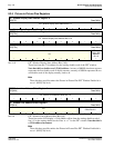
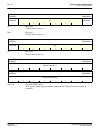
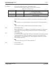
General Purpose IO Pins Configuration Register 1
REG[A9h] Read/Write
GPIO Pin
Input Enable
n/a
7 6 5 4 3 2 1 0
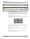
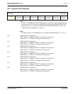
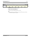
General Purpose IO Pins Status/Control Register 0
REG[ACh] Read/Write
n/a
GPIO6 Pin IO
Status
GPIO5 Pin IO
Status
GPIO4 Pin IO
Status
GPIO3 Pin IO
Status
GPIO2 Pin IO
Status
GPIO1 Pin IO
Status
GPIO0 Pin IO
Status
76543210