


Epson Research and Development Page 33
Vancouver Design Center
Hardware Functional Specification S1D13708
Issue Date: 02/03/07 X39A-A-001-02
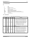
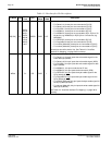
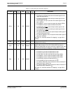
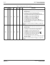
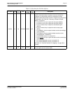
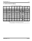
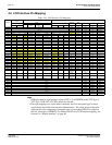
WAIT# O L8 PBCC8C IOVDD Hi-Z
During a data transfer, this output pin is driven active to force the
system to insert wait states. It is driven inactive to indicate the
completion of a data transfer. WAIT# is released to the high
impedance state after the data transfer is complete. Its active polarity
is configurable. See Table 4-8: “Summary of Power-On/Reset
Options,” on page 38.
• For Generic #1, this pin outputs the wait signal (WAIT#).
• For Generic #2, this pin outputs the wait signal (WAIT#).
• For SH-3 mode, this pin outputs the wait request signal
(WAIT#).
• For SH-4 mode, this pin outputs the device ready signal
(RDY#).
• For MC68K #1, this pin outputs the data transfer acknowledge
signal (DTACK#).
• For MC68K #2, this pin outputs the data transfer and size
acknowledge bit 1 (DSACK1#).
• For REDCAP2, this pin is unused (Hi-Z).
• For DragonBall, this pin outputs the data transfer acknowledge
signal (DTACK
).
• For Indirect (Mode 68), this pin is unused (Hi-Z).
• For Indirect (Mode 80), this pin is unused (Hi-Z).
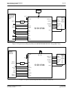
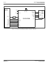
See Table 4-9: “Host Bus Interface Pin Mapping,” on page 39
for
summary.
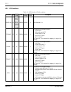
RESET# I A2 PICS IOVDD 0
Active low input to set all internal registers to the default state and to
force all signals to their inactive states.
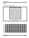
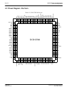
Table 4-3: Host Interface Pin Descriptions
Pin Name Type
PFBGA
Pin #
Cell
IO
Voltage
RESET
# State
Description