


Epson Research and Development Page 137
Vancouver Design Center
Hardware Functional Specification S1D13708
Issue Date: 02/03/07 X39A-A-001-02
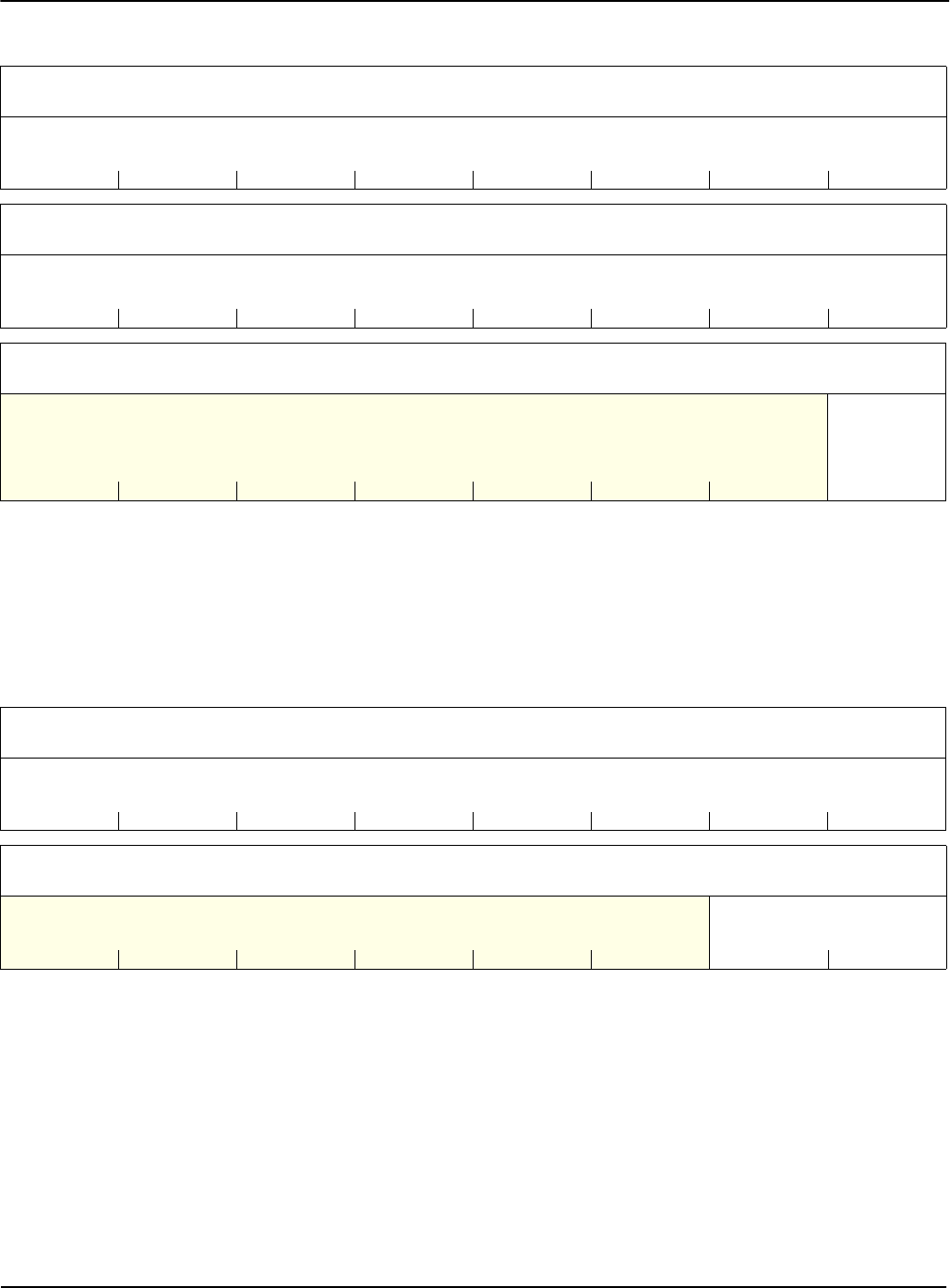
bits 16-0 Main Window Display Start Address Bits [16:0]
These bits form the 17-bit address for the starting double-word of the LCD image in the
display buffer for the main window.
Note that this is a double-word (32-bit) address. An entry of 00000h into these registers
represents the first double-word of display memory, an entry of 00001h represents the sec-
ond double-word of the display memory, and so on.
bits 9-0 Main Window Line Address Offset Bits [9:0]
These bits are the LCD display’s 10-bit address offset from the starting double-word of
line “n” to the starting double-word of line “n + 1” for the main window. Note that this is
a 32-bit address increment.
A virtual image can be formed by setting this register to a value greater than the width of
the main window. The displayed image is a window into the larger virtual image.
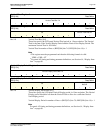
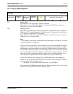
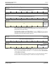
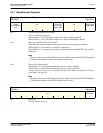
Main Window Display Start Address Register 0
REG[74h] Read/Write
Main window Display Start Address Bits 7-0
76543210
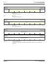
Main Window Display Start Address Register 1
REG[75h] Read/Write
Main window Display Start Address Bits 15-8
76543210
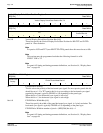
Main Window Display Start Address Register 2
REG[76h] Read/Write
n/a
Main window
Display Start
Address
Bit 16
7 6 5 4 3 2 10
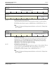
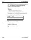
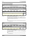
Main Window Line Address Offset Register 0
REG[78h] Read/Write
Main window Line Address Offset Bits 7-0
76543210
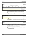
Main Window Line Address Offset Register 1
REG[79h] Read/Write
n/a
Main window Line Address
Offset Bits 9-8
7 6 5 4 3 210