


Epson Research and Development Page 35
Vancouver Design Center
Hardware Functional Specification S1D13708
Issue Date: 02/03/07 X39A-A-001-02
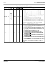
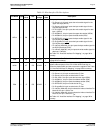
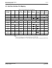
GPIO0 IO H10 PBCC8 IOVDD 0
This pin has multiple functions.
• PS for Sharp HR-TFT
• XINH for Epson D-TFD
• VCLK for TFT Type 2
• CPV for Type 3
• General purpose IO pin 0 (GPIO0)
• Hardware Video Invert
See Table 4-10: “LCD Interface Pin Mapping,” on page 40
for
summary.
GPIO1 IO J9 PBCC8 IOVDD 0
This pin has multiple functions.
• CLS for Sharp HR-TFT
• YSCL for Epson D-TFD
• AP for TFT Type 2
•OE for Type 3
• General purpose IO pin 1 (GPIO1)
See Table 4-10: “LCD Interface Pin Mapping,” on page 40
for
summary.
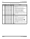
GPIO2 IO J10 PBCC8 IOVDD 0
This pin has multiple functions.
• REV for Sharp HR-TFT
• FR for Epson D-TFD
• POL for TFT Type 2
• POL for Type 3
• General purpose IO pin 2 (GPIO2)
See Table 4-10: “LCD Interface Pin Mapping,” on page 40
for
summary.
GPIO3 IO J11 PBCC8 IOVDD 0
This pin has multiple functions.
• SPL for Sharp HR-TFT
• FRS for Epson D-TFD
• STH for TFT Type 2
• EIO for Type 3
• General purpose IO pin 3 (GPIO3)
See Table 4-10: “LCD Interface Pin Mapping,” on page 40
for
summary.
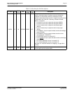
GPIO4 IO K10 PBCC8 IOVDD 0
This pin has multiple functions.
• RES for Epson D-TFD
•VCOM for Type 3
• General purpose IO pin 4 (GPIO4)
See Table 4-10: “LCD Interface Pin Mapping,” on page 40
for
summary.
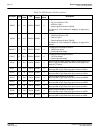
Table 4-4: LCD Interface Pin Descriptions
Pin Name Type
PFBGA
Pin #
Cell
IO
Voltage
RESET#
State
Description